By group chat requests, I started looking at emulating various e-learning devices manufactured by Noahedu.
NP7000 is a particularly interesting device, as it runs a fully custom NOAHOS operating system that I was always interested in reverse engineering, and it uses Ingenic SoC with available documentation and I have prior experiences working with and emulating them.
Emulation is done using a patched version QEMU to support various Ingenic peripherals, here is the relevant wiki page I wrote:
https://github.com/OpenNoah/OpenNoah.github.io/wiki/NP7000-Emulation
Identifying SoC chip model
This is rather easy with NP7000.
Simply download one of its full (TF-card) firmware upgrade package, still available here:
https://downloads.youxuepai.com/source/list.shtml#107-2361-0-0-0-0-0-0-
Extract it, the V3.2 firmware package consists of 4 files:
1 | ls |
Open the .idx file in a hex editor, then it is immediately visible:
1 | hexedit NP7000\(INAND\ V3.2\).idx |
Extracting ASCII strings from .idx and .mop also shows JZ4755:
1 | strings NP7000\(INAND\ V3.2\).idx | grep JZ4 |
So, most definitely the SoC chip is Ingenic JZ4755.
Here are some datasheets relevant to the JZ4755 SoC:
https://opennoah.github.io/datasheet/JZ4755_DS.PDF
https://opennoah.github.io/datasheet/JZ4755_pm.pdf
https://opennoah.github.io/datasheet/XBurst1_Core_PM.pdf
https://opennoah.github.io/datasheet/X1000_M200_XBurst_ISA_MXU_PM.pdf
MIPS basic
A couple of basic MIPS knowledge you should know.
kseg memory mapping
https://training.mips.com/basic_mips/PDF/Memory_Map.pdf
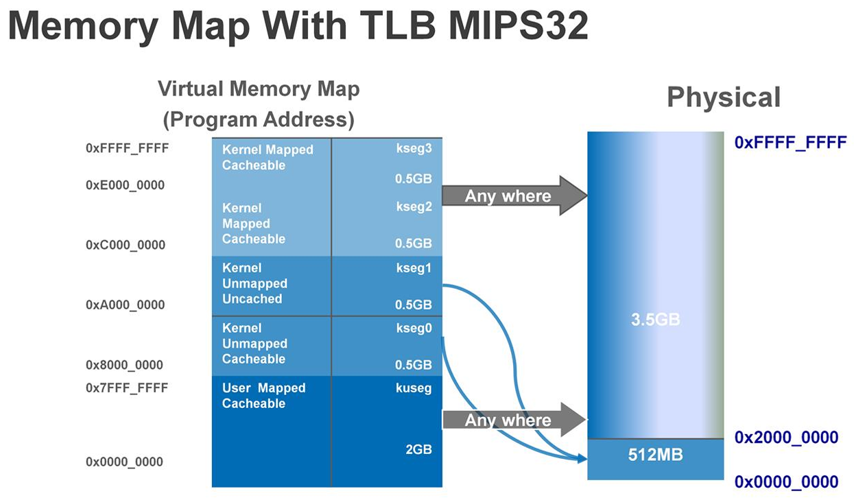
kseg0 region of size 0x20000000 starting from offset 0x80000000 and kseg1 at 0xa0000000 both maps to hardware physical address offset from 0x00000000, the only difference being cache-ability.
In the JZ4755 datasheet, the register addresses are shown in the physical address space like 0x1002101c.
To access the register from kernel driver code, we use the kseg1 address space, as that region is uncached.
So, for example, hardware register at 0x1002101c would be accessed using address 0xa0000000 + 0x1002101c = 0xb002101c.
First stage boot loader
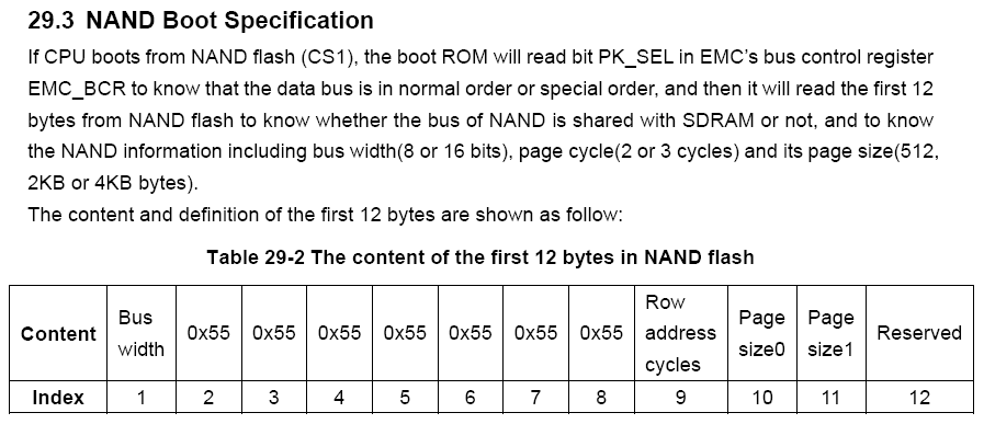
According to JZ4755 programming manual, section 29 XBurst Boot ROM Specification, JZ4755 supports booting from either NAND flash or SD card connected to the MSC0 controller.
In either cases, it loads 8 KiB data into internal SRAM offset 0x80000000.
Section 29.2 Boot Sequence:
NOTE: The JZ4755 internal SRAM is 16KB, its address is from 0x80000000 to 0x80004000.
(Actually I suspect the SRAM may be implemented simply by re-using the CPU data cache?)
Take a look at the .mop file:
1 | hd NP7000\(INAND\ V3.2\).mop | less |
Data starting from offset 0x00001bf0 up to 8 KiB offset 0x00002000 are all 0xff, usually used as NAND fill pattern when data is not present, as that is usually the data bytes in NAND after erasing.
So, this 8 KiB data section is very likely the first stage boot loader.
Also notice that the first 12 bytes of this data section does not have repeating 0x55 bytes, so this cannot be a NAND boot sequence, content does not match:
So, we know this must be loaded from MSC0 into offset 0x80000000, and CPU entry is also at offset 0x80000000.
We have seen similar implementations from Noahedu’s previous devices, e.g. the NP6800 is also using a flash controller chip to use a NAND chip as a SD card as its internal storage, much like the morden day eMMC storage solutions:
https://github.com/OpenNoah/OpenNoah.github.io/wiki/NP6800+-Gallery
Extract this data section to a separate file using dd:
1 | dd if="NP7000(INAND V3.2).mop" of=boot_1st.bin bs=1024 count=8 |
The next 8 KiB section has exactly the same data as the first one.
The NAND boot sequence does support having a backup section like this, in case data from the first section was corrupted. However, as the device is booting from SD card, this is unused.
Load it into Ghidra.
Set language as MIPS, default variant, 32-bit, little endian, eabi compiler.
In options, set base address to 0x80000000.
Immediately, disassembled code looks reasonable, there are a few prints, we can guess some function names:
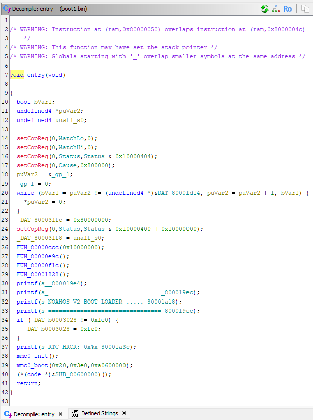
(All the custom names are added by me manually.)
Looking at the print functions, we can find that it eventually writes to register address 0xb0031000, that means it prints logs to UART1.
Usually the first stage boot loader configures SDRAM controller, so that it can load much more data from non-volatile storage and start executing the more complex next stage boot code.
Look inside the mmc0_boot(0x20,0x3e0,0xa0600000) function:
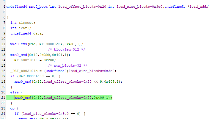
Pretty standard SD card initialisation code.
SD card specification can be downloaded from:
https://www.sdcard.org/downloads/pls/
Part 1 Simplified Physical Layer Simplified Specification
A few notable lines from the disassembled code:
1 | // Inside mmc0_boot(0x20,0x3e0,0xa0600000) |
1 | // Back to the entry() code |
So that means, it loads 0x3e0 * 512 = 496 KiB data from MSC0 offset 0x20 * 512 = 16 KiB into 0x80600000.
Second stage boot loader
Extract the section stage data from the .mop file:
1 | dd if="NP7000(INAND V3.2).mop" of=boot_2nd.bin bs=1024 skip=16 count=496 |
1 | hd NP7000\(INAND\ V3.2\).mop | less |
Similar to previous boot stage, all 0xff from 0x000154c0 up to 0x00080000 (512 KiB offset).
So, this section also looks plausible.
Again, load into Ghidra, mips 32-bit little-endian but at offset 0x80600000 instead.
Interesting code starting around offset 0x80605038:
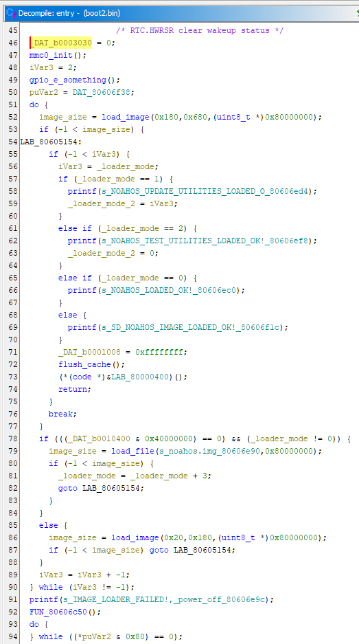
Function at 0x80604e5c:
Function at 0x80603fbc:
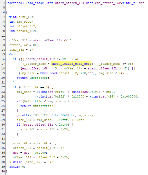
Reading the code, again we can find the mmc0_read() code to read data from MSC0, then calculate the parameters of the load_image() are using 16 KiB block sizes.
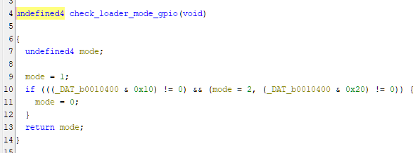
Register address 0xb0010400 is the PIN input register of GPIO group PE.
We can read from the code that it supports a few different booting modes:
- Normal boot, starting block offset
0x180 = 6 MiB, max number of blocks0x680 = 26 MiB - Update utilities, starting block offset
0x20 = 512 KiB, max number of blocks0x180 = 6 MiB, enabled byPE4 == 0 - Test utilities, same starting block offset
0x20 = 512 KiB, max number of blocks0x180 = 6 MiB, enabled byPE5 == 0 MSC1SD card boot fromnoahos.imgfile, enabled byPE30 == 0
And we can read that load address is 0x80000000, entry address is 0x80000400.
Number of blocks is recorded as 4 bytes located at offset 0x01f0 in the first block.
However, looking at .mop file offset 0x00600000 = 6 MiB, the data is not on a clear boundary:
1 | 005FFFC0 07 00 65 88 40 02 A2 27 38 02 A7 A3 04 00 65 98 03 00 46 A8 0B 00 67 88 00 00 46 B8 44 02 A2 27 ..e.@..'8.....e...F...g...F.D..' |
And if I try to boot the .mop file in MSC0 as-is, it simply gets stuck after these prints:
1 | ======================================= |
We can confirm that the bytes at offset 0x006001f0 is indeed 0xa3a802c8.
Special kernel
So, we need to look into the firmware update utility to understand how to correctly parse the firmware upgrade package.
Fortunately booting the special function kernel looks much more promising:
1 | ======================================= |
Ok, for some reason it seems to have a NAND driver and is trying to read from non-existent NAND, so that failed.
So, extract the kernel binary from offset 0x00080000 (512 KiB) and size 0x00200000 (2 MiB), then load it into Ghidra at offset 0x80000000.
Create a function at offset 0x80000400 as that is the entry address.
Again reading the function at 0x8000237c:
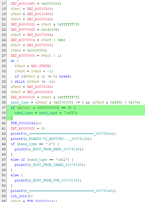
Satisfying condition (0xb0010200 & 0x80000000) == 0 i.e. GPIO PC31 == 0 makes it boot from MSC0 SD card instead of NAND.
So that’s what Noahedu means by “INAND”.
Fixing that in the emulator, now we get:
1 | ======================================= |
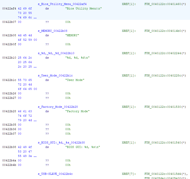
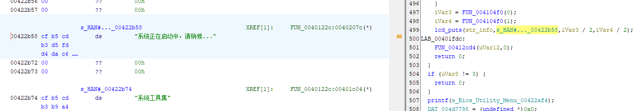
Looking at strings found by Ghidra, we can find strings that got printed to UART like:Bios Utility Menu
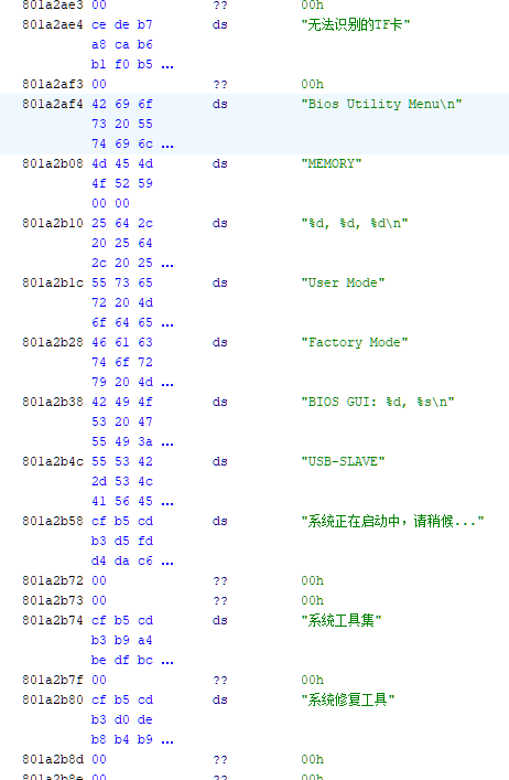
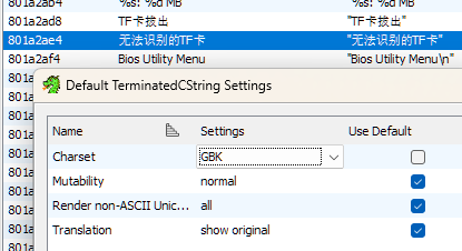
To decode Chinese strings, set default charset to GBK or GB2312, then set the relevant data section data type as TerminatedCString:
It is strange that Ghidra cannot find any references to these strings, there must be further logic to be understood.
There is likely another binary executable embedded in there and loaded by the kernel to a different address, especially these log prints look suspicious:
1 | Logo package size:1777640 |
Looking back at the .mop file data, I found that earlier offset 0x00200000 appears to be a starting location of a new data section, as it’s a new set of data just after a bunch of 0xff bytes:
1 | 001FFFC0 FF FF FF FF FF FF FF FF FF FF FF FF FF FF FF FF FF FF FF FF FF FF FF FF FF FF FF FF FF FF FF FF ................................ |
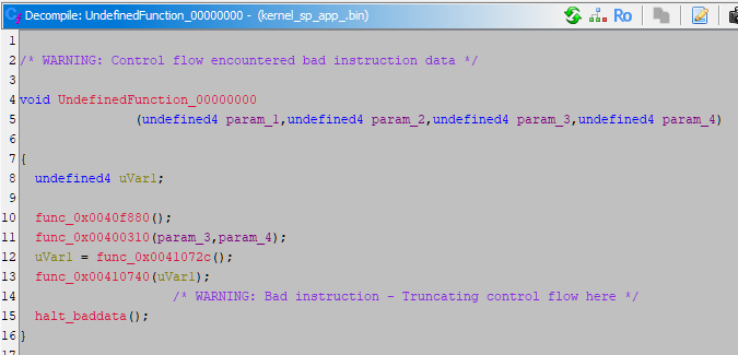
Load it into Ghidra with address offset set to 0 as I did not know the correct value yet, I can see some failed references:
Based on the function addresses it references, it seems very likely that the load address should be 0x00400000 instead.
And indeed, after fixing the address, Ghidra disassembly looks much better:
And there are now references to these strings we found earlier:
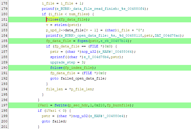
After some more painful reverse engineering of that executable, I finally located a few functions used for firmware upgrade, at 0x00406990, 0x00407cf4 and 0x00407448:
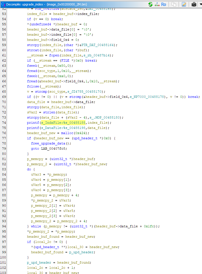
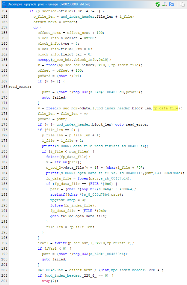
From these functions I understood how it parses the .idx index file, and .mop, .mo1 etc. data files.
It can take an arbitrary number of data files, it simply overwrites the file suffix with a number.
Here are the most important header fields, all integers are unsigned 32-bit little-endian:

From these information, finally I can re-construct a full system image.
Main kernel now boots, except for a segmentation fault in QEMU because of a bug in emulating the Ingenic Q16ADD MXU1 instruction, which was easy to fix.
1 | ======================================= |
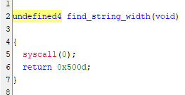
Syscall, syscall and more syscalls
Whilst looking at the firmware update program, I found that it does not operate on the storage device directly.
Instead, it does a bunch of syscalls with the file '\\DEVICE\BURNFILE'.
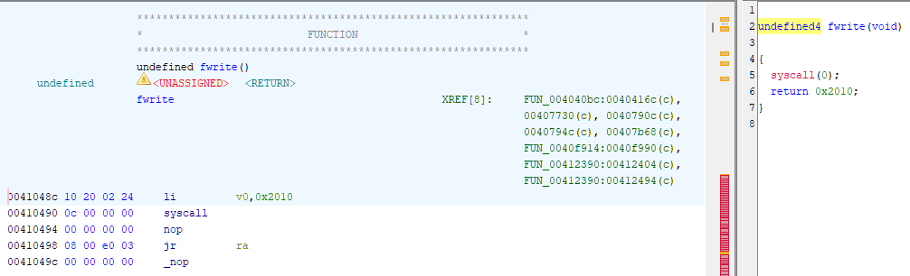
Inferring from the usage of the syscall functions, they look like standard file access functions e.g. fopen, fwrite, fread, fclose.
The syscall function itself does not do any operation on the registers, so Ghidra is unable to infer things like number of function arguments and return type. It simply triggers a syscall interrupt then nothing else.
I was also looking at LCD screen operations, since I didn’t have it working in the emulator yet, that’s the main thing I was looking to fix.
Again, following the text strings to LCD print functions, the main functionalities are hidden behind syscalls.
So now, we need to go back to the kernel to understand what the syscalls are actually doing.
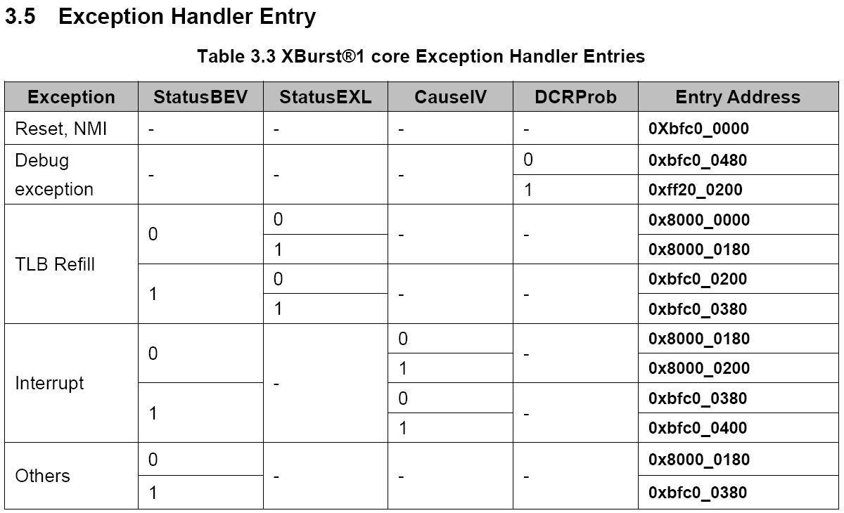
Syscalls should trigger an interrupt in the kernel, details about interrupts are described in the CPU programming manual, section 3 Exceptions.
The Ingenic documentation isn’t very clear, I believe Status.BEV == 0 and Cause.IV == 0 for the kernel, so exception handler entry address should be at 0x80000180.
Back to the kernel and start disassemble at that address, an exception handler appears:
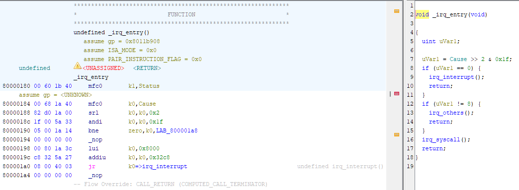
Following the syscall handler logic, it uses an array of arrays of pointer to look up the function to process syscalls.
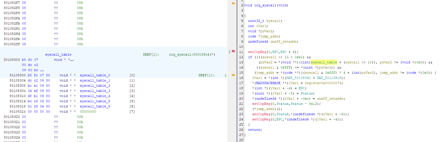
Finally, we can figure out what operations are actually happening.
LCD framebuffer and Ingenic MXU
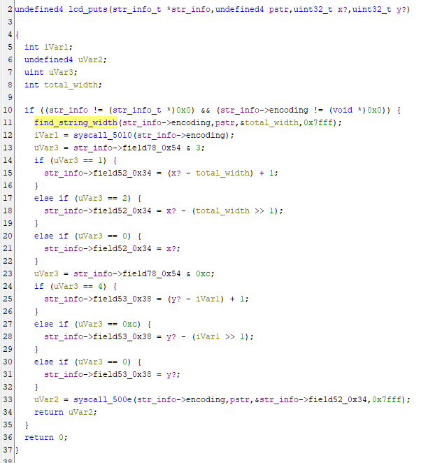
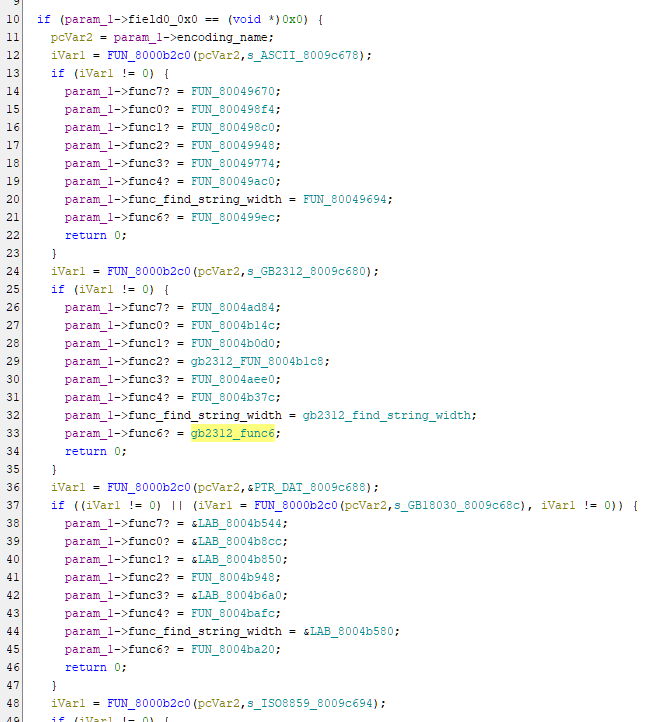
The functions to put some text on the screen are quite complicated to analyse, as it supports multiple different encodings and fonts.
The data structures used to store these information are rather complex.
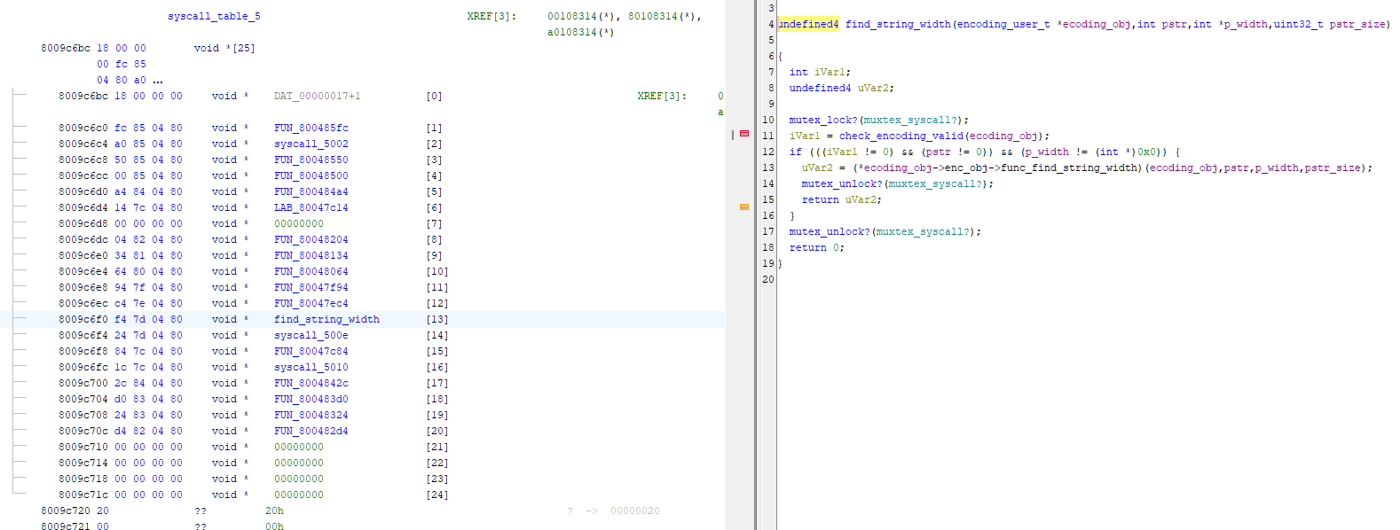
Eventually I figured out that syscall 0x4002 is the function to update LCD framebuffer after screen updates all completed.
Being able to use QEMU to run the actual code, set breakpoints, single step through instructions and looking at memory content is super helpful on doing the analysis.
I can also add debug logs on LCD controller emulation to show the actual physical addresses of the framebuffer:
1 | 2026-05-07T23:18:15.076780Z ingenic_lcd_enable 1 |
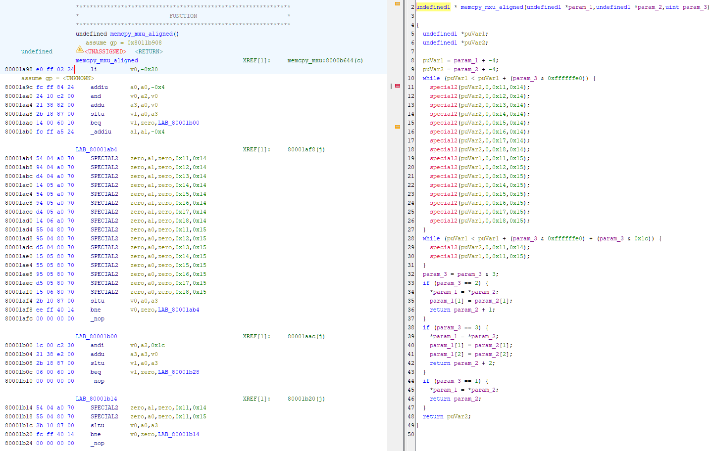
Inside syscall 0x4002, there is a memcpy-looking function at 0x80001a98:
Using gdb attached to QEMU, we can check its three parameters in registers a0, a1 and a2:
1 | (gdb) b *0x80001a98 |
a0 = 0x80742000 matches the LCD framebuffer physical address dsa=0x742000, so this is indeed the function that updates LCD screen content.
Interestingly, there are instructions that Ghidra could not understand, mnemonics listed as SPECIAL2.
gdb also could not understand them:
1 | B+>0x80001a98 li v0,-32 |
Even QEMU, which does support executing those Ingenic MXU instructions, does not support their mnemonics in in_asm logs:
1 | # qemu -d in_asm,op |
These must be the special Ingenic MXU instructions, we can try to decode it manually from the documentation.
Documentation for this is also not very good, but usable enough.
1 | 80001ab4 54 04 a0 70 SPECIAL2 zero,a1,zero,0x11,0x14 |
So, instruction is S32LDI or S32LDIR:
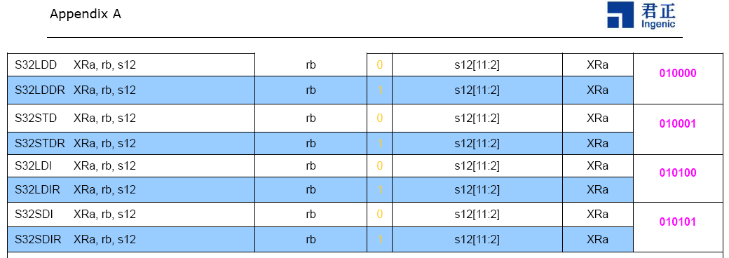
From the other table in the document we can find out the bit widths of other instruction fields:
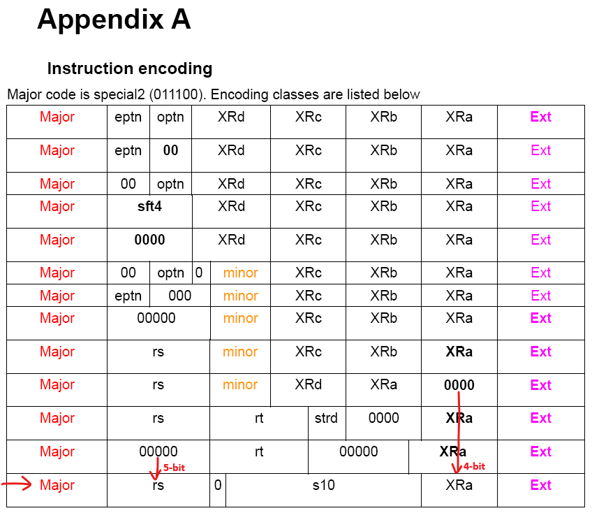
1 | Instruction = 01110000 10100000 00000100 01010100 |
Now we know the instruction is S32LDI, we can check its function from the document:
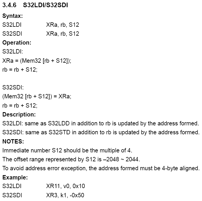
So basically loading data from memory to a MXU special register and incrementing the pointer register at the same time.
Later instructions like this S32SDI then writes it to the destination address:
1 | 80001ad4 55 04 80 70 SPECIAL2 zero,a0,zero,0x11,0x15 |
So this is just a special memcpy implementation that copies data using Ingenic MXU instructions.
Anyway, I figured out the issue with my LCD emulation, just a stupid error that framebuffer address wasn’t calculated correctly for the special 4bpp palette + RGB565 OSD overlay mode, basically repeating the first line for the whole screen.
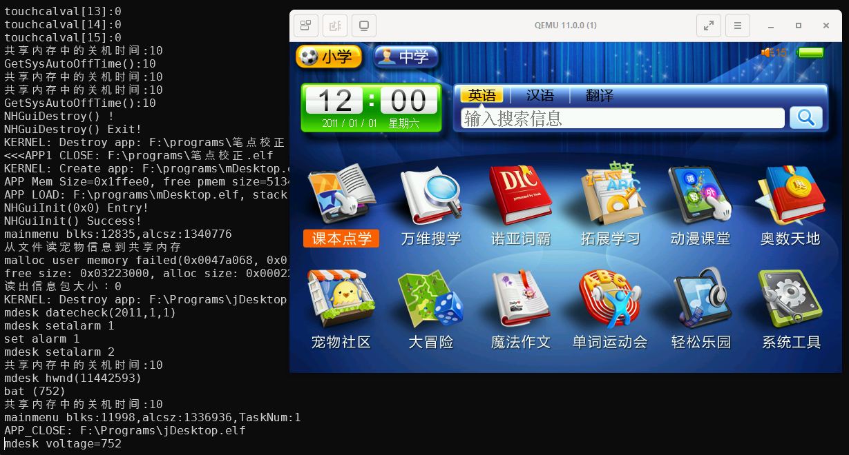
Finally I’m able to boot the NP7000 in QEMU and see its display: